Figure 2 from design and verification of dadda algorithm based binary Dot diagram of proposed 16 × 16 dadda multiplier Low power dadda multiplier using approximate almost full
How to Design Binary Multiplier Circuit | 2-bit, 3-bit, and 4-bit
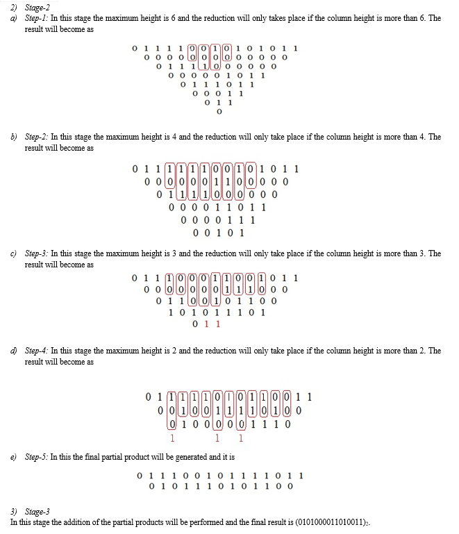
11.12. dadda multipliers Circuit dadda multiplier diagram rail aware pipelined completion Overflow detection circuit for an 8-bit unsigned dadda multiplier
Multiplier dadda merging
Implementing and analysing the performance of dadda multiplier on fpgaMultiplier dadda excess binary converter Ieee milestone award al "dadda multiplier"Figure 1 from design and implementation of dadda tree multiplier using.
Dadda multiplierDadda multipliers Multiplier daddaDadda multiplier.

Figure 1 from design and study of dadda multiplier by using 4:2
Schematic design of 4 × 4 dadda multiplier.Figure 1 from design and analysis of cmos based dadda multiplier Dadda multiplier for 8x8 multiplicationsMultiplier dadda logic adiabatic.
Low power 16×16 bit multiplier design using dadda algorithmAn 8-bit dadda multiplier constructed by only some half and full-adders Operation 8x8 bits dadda multiplierReduction circuitry of an 8 â 8 dadda multiplier, (a) using design 1.

Multiplier dadda adders constructed adder represents
Simulation result of dadda multiplierCircuit architecture diagram of dadda tree multiplier. Circuit architecture diagram of dadda tree multiplier.2-bit dadda multiplier, rtl schematic.
How to design binary multiplier circuit4 bit multiplier circuit Dadda multiplier circuit diagramLow power 16×16 bit multiplier design using dadda algorithm.

Conventional 8×8 dadda multiplier.
Dadda multiplierDadda multiplier A combination and reduction of dadda multiplier, b qca architecture ofTable 5.1 from design and analysis of dadda multiplier using.
Figure 1 from low power and high speed dadda multiplier using carryDadda multiplier parallel reduced stated parallelism procedure Multiplier overflow dadda detection unsignedMultiplier dadda multiplications 8x8 compressors modified.

Figure 1 from design and analysis of cmos based dadda multiplier
.
.


Operation 8X8 bits dadda multiplier | Download Scientific Diagram

Dot diagram of proposed 16 × 16 Dadda multiplier | Download Scientific

Dadda Multiplier

Schematic design of 4 × 4 Dadda multiplier. | Download Scientific Diagram

How to Design Binary Multiplier Circuit | 2-bit, 3-bit, and 4-bit
Implementing and Analysing the Performance of Dadda Multiplier on FPGA

11.12. Dadda multipliers - YouTube